Silicon carbide (SiC) crystal structure represents a cornerstone material in advanced industrial applications, driving innovation across electronics, automotive, energy, and aerospace sectors. For B2B buyers operating in diverse international markets—especially in Africa, South America, the Middle East, and Europe—understanding the nuances of SiC crystal structure is essential to securing high-performance, reliable components that meet stringent quality and cost requirements.
The unique properties of silicon carbide, including exceptional thermal conductivity, mechanical strength, and chemical stability, are intrinsically linked to its crystal structure. Variations in polytypes and crystal quality directly influence device efficiency and longevity, making crystal structure knowledge a critical factor in supplier selection and procurement strategy. This guide offers a comprehensive overview tailored to the complexities faced by global buyers, addressing everything from the fundamental types of SiC crystals and their material characteristics to manufacturing processes and quality control standards.
Additionally, the guide navigates the global supply landscape, highlighting key suppliers, cost drivers, and market trends that impact sourcing decisions. Practical insights into regulatory considerations and logistics further equip buyers to optimize their procurement workflows. Whether you are sourcing for semiconductor fabrication in Germany, industrial applications in South America, or energy solutions in the Middle East, this resource empowers you to make informed, strategic decisions that enhance product performance and cost-efficiency.
By combining technical depth with market intelligence, this guide serves as an indispensable tool for international B2B buyers seeking to master the complexities of silicon carbide crystal structure and secure competitive advantage in an evolving global marketplace.
| Type Name | Key Distinguishing Features | Primary B2B Applications | Brief Pros & Cons for Buyers |
|---|---|---|---|
| 3C-SiC (Cubic) | Zinc blende cubic crystal structure, isotropic properties | High-frequency electronic devices, power modules | Pros: Uniform electrical properties, easier wafer fabrication Cons: Lower thermal conductivity than hexagonal types |
| 4H-SiC (Hexagonal) | Hexagonal structure with 4 layers in stacking sequence | High-power electronics, LEDs, semiconductor wafers | Pros: High electron mobility, excellent thermal conductivity Cons: More complex growth process, higher cost |
| 6H-SiC (Hexagonal) | Hexagonal structure with 6 layers, stable and widely used | High-voltage devices, power electronics, sensors | Pros: Mature technology, good mechanical strength Cons: Lower electron mobility than 4H, less efficient for fast-switching |
| 15R-SiC (Rhombohedral) | Rhombohedral stacking, less common polytype | Specialized high-temperature and power applications | Pros: High thermal stability, unique electrical properties Cons: Limited availability, niche market |
| Amorphous SiC | Non-crystalline, lacks long-range order | Coatings, thin films, MEMS devices | Pros: Flexibility in deposition, good chemical resistance Cons: Poor electronic properties compared to crystalline types |
3C-SiC (Cubic Silicon Carbide):
3C-SiC features a cubic zinc blende structure that offers isotropic electrical properties, making it attractive for high-frequency electronic components and power modules. Its uniformity simplifies wafer fabrication, which can reduce manufacturing costs. However, its thermal conductivity is lower than hexagonal polytypes, which may limit performance in high-heat environments. Buyers should consider 3C-SiC when uniform electrical behavior and cost efficiency are priorities, especially for RF and microwave applications.
4H-SiC (Hexagonal Silicon Carbide):
4H-SiC is the most widely used hexagonal polytype, known for its superior electron mobility and excellent thermal conductivity. These characteristics make it ideal for high-power electronics, LEDs, and semiconductor wafers. However, the growth process for 4H-SiC is complex and more expensive, affecting procurement costs. B2B buyers should weigh the performance benefits against budget constraints, especially in industries demanding high efficiency and thermal management like automotive and renewable energy sectors.
6H-SiC (Hexagonal Silicon Carbide):
6H-SiC has a stable hexagonal structure with six layers in its stacking sequence, offering good mechanical strength and mature manufacturing processes. It is commonly used in high-voltage power devices and sensors. While it provides robust performance, its electron mobility is lower than 4H-SiC, which might reduce switching speeds. Buyers targeting reliable, cost-effective power electronics with established supply chains will find 6H-SiC a dependable choice.
15R-SiC (Rhombohedral Silicon Carbide):
The 15R polytype is less common and features a rhombohedral crystal structure, delivering high thermal stability and unique electrical properties. It is suitable for specialized applications requiring operation in extreme conditions, such as high-temperature power devices. Due to limited availability and niche demand, procurement might be challenging. Buyers should evaluate their application’s specific requirements and consider supplier capabilities when sourcing 15R-SiC.
Amorphous Silicon Carbide:
Unlike crystalline forms, amorphous SiC lacks long-range order, providing flexibility in thin film and coating applications. It offers excellent chemical resistance and is widely used in MEMS devices and protective coatings. However, its electronic properties are inferior to crystalline SiC, limiting its use in semiconductor applications. Buyers interested in surface protection and microfabrication should consider amorphous SiC for cost-effective, versatile solutions.
Related Video: INTERESTING MATERIALS: Silicon carbide
| Industry/Sector | Specific Application of silicon carbide crystal structure | Value/Benefit for the Business | Key Sourcing Considerations for this Application |
|---|---|---|---|
| Power Electronics | High-voltage, high-temperature semiconductor devices | Enhanced efficiency, reduced energy loss, improved thermal management | Purity, crystal defect density, wafer size compatibility with device manufacturing |
| Automotive | Electric vehicle (EV) powertrain components and inverters | Increased power density, longer component lifespan, better heat tolerance | Compliance with automotive standards, consistency in crystal quality, supplier reliability |
| Aerospace & Defense | High-performance sensors and RF devices for harsh environments | Superior durability, high-frequency operation, resistance to radiation and thermal stress | Certification for aerospace use, traceability, and material performance validation |
| Industrial Manufacturing | Abrasive and cutting tools based on SiC crystals | Higher hardness, wear resistance, and longer tool life | Crystal size, hardness grade, and supplier capacity for bulk orders |
| Renewable Energy | SiC-based power modules for solar inverters and wind turbines | Improved conversion efficiency, reduced cooling requirements, increased system reliability | Long-term supply agreements, product certification, and quality consistency |
Silicon carbide’s crystal structure is pivotal in power electronics, where it enables the production of semiconductor devices that operate efficiently at high voltages and temperatures. For B2B buyers in regions like Europe and Australia, sourcing SiC wafers with minimal crystal defects and appropriate wafer diameters is critical to ensure compatibility with advanced manufacturing processes. These materials significantly reduce energy losses and thermal management costs, directly impacting operational efficiency and product reliability.
In the automotive sector, particularly for electric vehicles, silicon carbide crystal structure is utilized in powertrain inverters and converters. This application demands crystals with consistent quality and strict adherence to automotive industry standards to withstand harsh operating conditions and deliver higher power density. Buyers from South America and the Middle East should prioritize suppliers with proven track records in automotive-grade SiC to reduce risks associated with performance variability.
The aerospace and defense industry benefits from silicon carbide’s robustness in fabricating high-frequency sensors and RF devices that function reliably in extreme environments. The crystal’s radiation resistance and thermal stability are essential for mission-critical applications. International buyers must ensure that suppliers provide full traceability and certification to meet stringent aerospace regulations, which is particularly important for companies in Africa and Europe engaged in defense contracts.
In industrial manufacturing, SiC crystals are integral to producing abrasive and cutting tools due to their exceptional hardness and wear resistance. Buyers need to focus on crystal size and hardness grade to match specific machining requirements. For bulk procurement, especially by manufacturers in South America and Africa, assessing supplier capacity and consistency is vital to maintain uninterrupted production cycles.
Finally, in the renewable energy sector, silicon carbide-based power modules are increasingly used in solar and wind energy conversion systems. These modules offer improved efficiency and reliability while lowering cooling system costs. Buyers from Europe and the Middle East should consider long-term supply agreements and product certifications to ensure stable supply and compliance with international quality standards, facilitating smooth integration into energy projects.
Related Video: What is Silicon Carbide?
Key Properties:
6H-SiC is characterized by a hexagonal crystal structure with excellent thermal conductivity (around 4.9 W/cm·K) and high breakdown electric field strength. It withstands high temperatures up to 1600°C and exhibits outstanding chemical inertness, making it highly resistant to oxidation and corrosion.
Pros & Cons:
- Pros: Exceptional thermal and chemical stability, high mechanical strength, and good electrical properties for power electronics.
- Cons: More complex and costly to manufacture due to its anisotropic crystal growth, which can lead to defects affecting yield.
Impact on Application:
Ideal for high-power, high-frequency semiconductor devices and harsh environment sensors. Its corrosion resistance suits chemical processing industries handling aggressive media.
International B2B Considerations:
Buyers in Europe (notably Germany) and Australia often require compliance with ASTM C1277 and DIN EN standards for semiconductor-grade SiC. In the Middle East and South America, where industrial chemical processing is growing, 6H-SiC’s robustness aligns well with local industrial needs. Africa’s emerging electronics sectors may prioritize cost-effective sourcing, so balancing quality and price is critical.
Key Properties:
3C-SiC has a cubic zinc blende crystal structure, offering higher electron mobility than hexagonal forms and a wide bandgap (~2.3 eV). It performs well under moderate thermal stress (up to ~1400°C) and has good chemical resistance, although slightly less than 6H-SiC.
Pros & Cons:
- Pros: Easier to grow as thin films on silicon substrates, enabling cost-effective manufacturing of electronic devices. Higher electron mobility benefits high-speed device applications.
- Cons: Lower thermal stability and mechanical strength compared to hexagonal SiC, limiting use in extreme environments.
Impact on Application:
Widely used in microelectronics and optoelectronics, especially for devices requiring integration with silicon technology. Suitable for applications with moderate temperature and chemical exposure.
International B2B Considerations:
European and Australian buyers value the compatibility of 3C-SiC with existing silicon-based manufacturing lines, facilitating integration and reducing costs. In South America and the Middle East, where semiconductor manufacturing is expanding, 3C-SiC offers a balance of performance and affordability. African buyers should verify compliance with JIS and ASTM standards to ensure quality and interoperability.
Key Properties:
4H-SiC is another hexagonal polytype with a wider bandgap (~3.26 eV) and superior electron mobility compared to 6H-SiC. It supports high temperature operation (up to 1700°C) and exhibits excellent chemical inertness and mechanical hardness.
Pros & Cons:
- Pros: Higher electron mobility and thermal conductivity than 6H-SiC, making it preferred for high-efficiency power devices and high-frequency applications.
- Cons: Manufacturing complexity and cost are higher due to precise control needed during crystal growth.
Impact on Application:
Dominates the power electronics market, especially for electric vehicles, renewable energy inverters, and industrial motor drives. Its robustness against harsh chemical environments also makes it suitable for aerospace and defense sectors.
International B2B Considerations:
European buyers, particularly in Germany, demand strict adherence to DIN and IEC standards for 4H-SiC to ensure reliability in automotive and energy sectors. Middle Eastern and South American buyers benefit from 4H-SiC’s efficiency gains in renewable energy projects. African markets should weigh the higher upfront cost against long-term performance benefits.
Key Properties:
Amorphous SiC lacks a long-range crystal order, resulting in lower thermal conductivity and mechanical strength but offering excellent chemical resistance and electrical insulation properties.
Pros & Cons:
- Pros: Easier and cheaper to produce in thin-film form, highly resistant to corrosion, and useful as protective coatings or dielectric layers.
- Cons: Lower mechanical and thermal performance restricts use in high-stress environments.
Impact on Application:
Commonly used as protective coatings in chemical processing equipment, biomedical devices, and MEMS technology where corrosion resistance is paramount but mechanical load is minimal.
International B2B Considerations:
Buyers in Africa and South America with emerging chemical and biomedical industries find a-SiC coatings cost-effective for extending equipment life. Europe and Australia prioritize compliance with ASTM and ISO standards for coating quality and environmental safety. The Middle East’s petrochemical sector benefits from its corrosion resistance but must consider long-term durability.
| Material | Typical Use Case for silicon carbide crystal structure | Key Advantage | Key Disadvantage/Limitation | Relative Cost (Low/Med/High) |
|---|---|---|---|---|
| 6H-SiC | High-power electronics, harsh chemical environments | Excellent thermal stability and chemical resistance | Complex manufacturing, higher cost | High |
| 3C-SiC | Microelectronics, optoelectronics, silicon integration | High electron mobility, cost-effective thin films | Lower thermal/mechanical stability | Medium |
| 4H-SiC | Power electronics, automotive, renewable energy | Superior electron mobility and thermal conductivity | High manufacturing complexity and cost | High |
| Amorphous SiC (a-SiC) | Protective coatings, biomedical devices, MEMS | Excellent corrosion resistance, low cost | Lower mechanical/thermal performance | Low |
This strategic material selection guide empowers international B2B buyers to align silicon carbide crystal structure choices with their specific industrial needs, regional standards, and cost-performance expectations.
Silicon carbide (SiC) crystal structures are foundational in high-performance electronics, power devices, and advanced ceramics. Understanding the manufacturing process is crucial for B2B buyers aiming to source high-quality SiC crystals that meet stringent industrial demands.
The process begins with raw material synthesis, typically involving high-purity silicon and carbon sources. These materials undergo purification to remove metallic and non-metallic impurities, which can adversely affect crystal quality. Advanced chemical vapor deposition (CVD) or sublimation techniques are used to ensure the feedstock’s chemical integrity.
The core manufacturing stage is the crystal growth, commonly executed through the Physical Vapor Transport (PVT) method, also known as sublimation growth. This involves heating silicon carbide powder at high temperatures (around 2500°C) in a graphite crucible within a controlled atmosphere to facilitate the deposition of SiC onto seed crystals. Other techniques, such as Chemical Vapor Deposition (CVD), may be employed to grow thin films or epitaxial layers with precise control over crystal orientation and doping.
Crystal orientation (e.g., 4H-SiC, 6H-SiC polytypes) and defect density are critical parameters monitored during growth, as they directly influence electrical and thermal properties.
Post-growth, the bulk crystals are sliced into wafers using diamond wire saws. These wafers undergo lapping and polishing to achieve the required surface finish and flatness essential for semiconductor device fabrication. Precision machining may be applied for shaping or dicing wafers into chips.
The finishing process includes cleaning, surface passivation, and sometimes doping or coating to enhance device performance. Packaging is tailored to protect the crystal structure during transport and integration into electronic modules, often involving moisture barriers and static shielding.
For B2B buyers, especially those from Africa, South America, the Middle East, and Europe, understanding quality assurance (QA) and control (QC) practices is key to selecting reliable suppliers and ensuring product consistency.
Quality control is embedded at multiple production stages to mitigate defects and maintain uniformity:
For international buyers, validating a supplier’s QC capabilities is essential to reduce risks and ensure product performance:
International buyers face distinct challenges and opportunities depending on their regional regulatory environments and industry expectations:
By focusing on these actionable insights, international B2B buyers can confidently navigate the complexities of sourcing silicon carbide crystal structures and foster partnerships with trustworthy manufacturers.
When sourcing silicon carbide crystal structures, understanding the underlying cost components is essential for effective budgeting and negotiation. The total cost typically comprises:
Several factors can cause price fluctuations or premium charges when sourcing silicon carbide crystal structures:
For buyers in Africa, South America, the Middle East, and Europe aiming to optimize cost-efficiency and total value, consider the following actionable insights:
Pricing for silicon carbide crystal structures varies widely depending on the factors outlined above. As such, any price indications should be treated as approximate and subject to negotiation and final contract terms. Buyers are advised to request detailed quotations from multiple suppliers and perform comprehensive cost comparisons before committing.
By applying these insights, international B2B buyers can navigate the complex cost and pricing landscape of silicon carbide crystal structures with greater confidence, achieving optimal value while mitigating risks inherent in global sourcing.
Understanding the critical technical properties of silicon carbide (SiC) crystal structures is essential for making informed procurement decisions. These properties directly affect the material’s performance, cost-efficiency, and suitability for specific industrial applications.
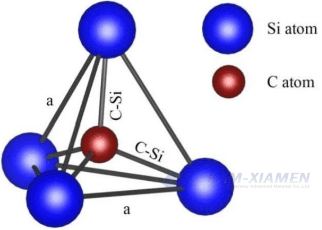
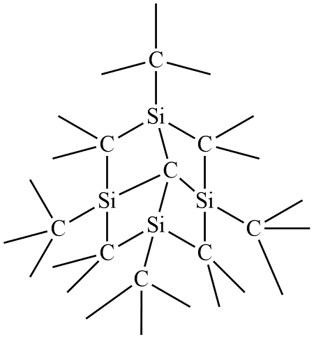
Polytype and Crystal Structure
Silicon carbide exists in multiple polytypes (e.g., 4H-SiC, 6H-SiC), which differ in their stacking sequences and electrical properties. For B2B buyers, selecting the correct polytype is crucial because it influences the material’s conductivity, thermal stability, and mechanical strength. For example, 4H-SiC is preferred for high-power electronic devices due to its superior electron mobility.
Material Grade and Purity
The grade refers to the purity and defect levels within the silicon carbide crystals. High-grade SiC exhibits fewer crystal defects and higher purity, which translates to better reliability and performance in semiconductor and high-temperature applications. Buyers should specify the required grade to ensure consistency and avoid costly production issues.
Dimensional Tolerance
This specifies the allowable deviation in size and shape from the nominal dimensions of the SiC crystals or wafers. Tight dimensional tolerances are vital for applications requiring precise fitting, such as semiconductor substrates or optical components. Understanding tolerance levels helps buyers negotiate specifications that balance quality with cost.
Electrical Resistivity
Electrical resistivity measures how strongly the SiC crystal opposes the flow of electric current. Different applications require different resistivity levels; for instance, power electronics demand materials with low resistivity for efficient conduction. Buyers should verify resistivity specifications to align with their product performance requirements.
Thermal Conductivity
Silicon carbide’s ability to conduct heat efficiently makes it highly desirable for high-temperature and high-power applications. Thermal conductivity values vary with crystal quality and polytype. Ensuring the supplier provides accurate thermal conductivity data helps buyers assess suitability for heat dissipation needs.
Mechanical Hardness and Fracture Toughness
SiC is known for its exceptional hardness and resistance to fracture, which makes it suitable for abrasive and structural applications. Buyers should consider these mechanical properties when selecting SiC for wear-resistant coatings or components subject to mechanical stress.
Familiarity with industry trade terms streamlines communication and negotiation, helping buyers from Africa, South America, the Middle East, and Europe navigate international transactions effectively.
OEM (Original Equipment Manufacturer)
Refers to companies that produce components or products used in another company’s end products. When sourcing SiC crystals, understanding whether the supplier is an OEM or a distributor can impact pricing, customization options, and lead times.
MOQ (Minimum Order Quantity)
The smallest quantity of SiC crystals a supplier is willing to sell in a single order. MOQs affect inventory planning and cost efficiency. Buyers should negotiate MOQs that align with their production scale to avoid excess inventory or supply shortages.
RFQ (Request for Quotation)
A formal document sent to suppliers to obtain pricing, lead times, and terms for specified quantities and product specifications. Issuing a clear RFQ with detailed technical requirements ensures accurate and comparable supplier responses.
Incoterms (International Commercial Terms)
Standardized trade terms defining the responsibilities of buyers and sellers for shipping, insurance, and tariffs. Common terms include FOB (Free On Board) and CIF (Cost, Insurance, and Freight). Understanding Incoterms helps buyers manage risk and control shipping costs effectively.
Lead Time
The period between placing an order and receiving the product. Lead times for silicon carbide crystals can vary based on complexity and supplier capacity. Accurate lead time knowledge is critical for production scheduling and meeting market demands.
Traceability
The ability to track the origin, manufacturing process, and quality control records of SiC crystals. Traceability is increasingly important for quality assurance and regulatory compliance, especially in sectors like automotive and aerospace.
By mastering these technical properties and trade terms, international buyers can make strategic decisions that optimize product performance, cost-efficiency, and supply chain reliability when sourcing silicon carbide crystal structures.
The silicon carbide (SiC) crystal structure market is experiencing robust growth driven by its expanding applications in power electronics, electric vehicles (EVs), renewable energy systems, and advanced semiconductor devices. Globally, demand is propelled by the increasing need for energy-efficient components that operate at high voltages, temperatures, and frequencies. For international B2B buyers in regions such as Africa, South America, the Middle East, and Europe—including industrial hubs like Germany and Australia—understanding these market forces is critical for strategic sourcing and supply chain resilience.
Key market drivers include:
For B2B buyers, it is essential to monitor market consolidation trends, strategic partnerships, and emerging suppliers offering competitive pricing and technical support. Leveraging digital procurement platforms that provide transparency on lead times, certification, and traceability can mitigate risks associated with volatile supply and demand cycles.
Sustainability is becoming a non-negotiable aspect of silicon carbide crystal sourcing, especially for buyers committed to corporate social responsibility and regulatory compliance. The production of SiC crystals involves energy-intensive processes and raw material extraction, which can generate significant environmental footprints.
Environmental considerations include:
Ethical sourcing is equally critical. Buyers from Africa, South America, and the Middle East should ensure their supply chains avoid conflict minerals and comply with international labor standards. Partnering with suppliers who hold certifications such as ISO 14001 (Environmental Management), REACH compliance, and RoHS directives helps guarantee adherence to environmental and social governance (ESG) criteria.
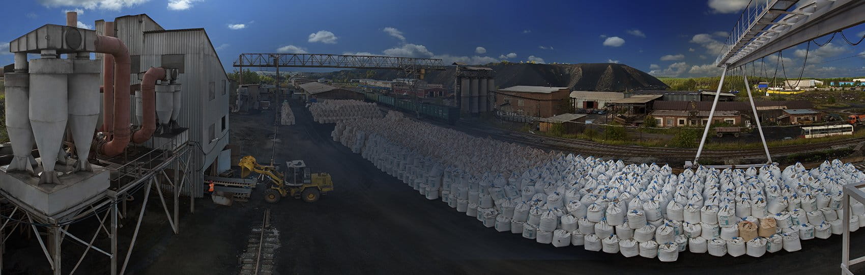
Illustrative Image (Source: Google Search)
Furthermore, “green” silicon carbide variants—produced via cleaner, low-waste processes—are emerging in the market. These products often come with lifecycle assessments (LCAs) and sustainability reports, enabling buyers to make informed procurement decisions aligned with global sustainability goals.
Illustrative Image (Source: Google Search)
Silicon carbide has a rich history dating back to the late 19th century when it was first synthesized as an abrasive material. However, its application in semiconductor technology and power electronics has only gained momentum over the past few decades. The development of high-purity, single-crystal SiC substrates in the 1980s and 1990s marked a pivotal evolution, enabling devices that outperform traditional silicon components in harsh environments.
For international B2B buyers, understanding this evolution underscores the importance of selecting suppliers with proven expertise in crystal growth and defect control. The transition from bulk SiC production to wafer-level fabrication has opened new opportunities in high-performance electronics, catalyzing strategic investments worldwide. This historical perspective informs sourcing strategies that balance cost, quality, and innovation, particularly in fast-growing industrial markets.
How can I effectively vet suppliers of silicon carbide crystal structures for international B2B transactions?
To vet suppliers, prioritize those with verifiable certifications such as ISO 9001 or industry-specific accreditations related to semiconductor materials. Request detailed technical datasheets and sample batches to assess quality firsthand. Check references and client testimonials, especially from buyers in your region, to gauge reliability. Consider suppliers with transparent production processes and robust quality control. For Africa, South America, the Middle East, and Europe, understanding the supplier’s export experience and compliance with international trade regulations is critical to avoid customs or regulatory delays.
What customization options are typically available for silicon carbide crystal structures, and how should I approach these with suppliers?
Silicon carbide crystals can be customized in terms of polytype, doping elements, wafer size, thickness, and orientation to meet specific application needs. Engage suppliers early with detailed technical requirements and intended end-use to ensure feasibility. Request prototypes or small trial orders to validate the custom specifications before scaling. For international buyers, clarify customization timelines and additional costs upfront, as these can impact lead times and pricing significantly, especially when sourcing from diverse regions like Europe or the Middle East.
What are the common minimum order quantities (MOQs) and lead times for silicon carbide crystal structures in international B2B trade?
MOQs vary widely depending on the supplier’s production scale and crystal specifications, often ranging from a few wafers to several hundred units. Lead times typically range from 4 to 12 weeks due to the complexity of crystal growth and post-processing. Buyers should negotiate MOQs early to align with project timelines and storage capabilities. For buyers in Africa and South America, consider additional transit times and customs clearance when planning orders. Establish clear communication on lead times to avoid production delays and optimize inventory management.
Which payment terms are standard when purchasing silicon carbide crystal structures internationally, and how can buyers mitigate financial risks?
Common payment terms include letters of credit (LC), advance payments, and net terms ranging from 30 to 90 days. Letters of credit provide security for both parties by guaranteeing payment upon delivery confirmation. For buyers in emerging markets, negotiating partial advance payments combined with escrow services can reduce risks. Always ensure contracts specify payment milestones aligned with quality inspections and shipment progress. Using reputable financial intermediaries and understanding the supplier’s banking practices in their country can further safeguard transactions.
What quality assurance certifications and testing standards should I expect from silicon carbide crystal structure suppliers?
Suppliers should provide certifications such as ISO 9001 for quality management and, where applicable, ISO/TS 16949 for automotive-grade materials or IEC standards for electronic components. Testing reports should include crystal purity, defect density, doping concentration, and electrical properties. Request third-party inspection or audit reports to verify claims. Consistent QA certifications ensure product reliability, which is crucial for high-performance applications. International buyers should verify that documentation meets their country’s import regulations and industry standards to prevent compliance issues.
How can I optimize logistics and shipping for silicon carbide crystal structures to regions like Africa, South America, the Middle East, and Europe?
Plan shipments with suppliers who have experience in international freight forwarding and can handle customs documentation efficiently. Silicon carbide wafers require careful packaging to prevent contamination and mechanical damage. Choose logistics partners familiar with handling sensitive semiconductor materials and capable of providing temperature-controlled shipping if necessary. Consider Incoterms carefully—CIF or DDP terms can reduce risk by shifting customs clearance responsibilities to the supplier. Early coordination with customs brokers and understanding import duties in your country will expedite delivery and reduce unexpected costs.
What steps should I take if a dispute arises regarding the quality or delivery of silicon carbide crystal structures?
First, document all communications, contracts, and inspection reports thoroughly. Engage the supplier promptly to discuss discrepancies and seek amicable resolution through negotiation or mediation. Ensure your purchase agreement includes clear dispute resolution clauses specifying jurisdiction and arbitration methods. If unresolved, consider involving third-party inspection agencies or legal counsel specializing in international trade law. Maintaining transparent communication channels and having a strong contract framework helps minimize disputes and expedites resolution, particularly in cross-border transactions.
Are there specific regional considerations for sourcing silicon carbide crystal structures from Europe, the Middle East, or emerging markets?
Yes, regional factors such as regulatory environments, export controls, and local industry maturity influence sourcing strategies. Europe, especially Germany, offers advanced manufacturing and stringent quality standards but may have higher costs. The Middle East is emerging as a strategic hub with increasing investment in semiconductor materials, but buyers should assess supplier stability and export compliance. In Africa and South America, infrastructure challenges and longer shipping times require contingency planning. Understanding local trade agreements, tariffs, and potential political risks ensures smoother procurement and supply chain continuity.
The information provided in this guide, including content regarding manufacturers, technical specifications, and market analysis, is for informational and educational purposes only. It does not constitute professional procurement advice, financial advice, or legal advice.
While we have made every effort to ensure the accuracy and timeliness of the information, we are not responsible for any errors, omissions, or outdated information. Market conditions, company details, and technical standards are subject to change.
B2B buyers must conduct their own independent and thorough due diligence before making any purchasing decisions. This includes contacting suppliers directly, verifying certifications, requesting samples, and seeking professional consultation. The risk of relying on any information in this guide is borne solely by the reader.
The strategic sourcing of silicon carbide crystal structures demands a nuanced understanding of material properties, supplier capabilities, and regional market dynamics. For B2B buyers across Africa, South America, the Middle East, and Europe, prioritizing suppliers with proven expertise in delivering high-purity, defect-minimized SiC crystals can significantly enhance product performance and reliability. Emphasizing long-term partnerships and supply chain transparency will mitigate risks associated with geopolitical fluctuations and raw material scarcity.
Key takeaways include:
Looking ahead, as silicon carbide continues to underpin advancements in electric vehicles, renewable energy, and telecommunications, buyers must remain agile in sourcing strategies. Investing in supplier innovation and collaborative R&D initiatives will unlock new performance benchmarks and cost advantages. International buyers are encouraged to engage proactively with emerging suppliers and leverage digital procurement tools to enhance visibility and responsiveness.

Illustrative Image (Source: Google Search)
By integrating strategic sourcing principles with market intelligence, organizations can secure a competitive edge in the evolving silicon carbide landscape and drive sustainable growth across their industrial value chains.
Tags: Black Silicon Carbide, White Fused Alumina, Brown Fused Alumina, Pink Fused Alumina, Black Fused Alumina